
The PapierLogiK concept aims to be a Paper Logic Key model for optimizing the choice of materials used to produce more sustainable technologies.
It basically favors the use of cellulose and organic-based resources for the product core, and only make use of more durable to synthetic finish and thin reinforcement cover. This will ensure to obtain the less impactful end of life for our consuming goods.
The papierlogik website was created in 2011 to provide open source resources, tools and methods to produce fast and furioulsy efficient elctronics based on the above model. The Original Sensors Fabrication kit provides innovative materials resources, while the tutorials, application examples and many other resources from this website will help you to build your own sensors and use them in a variety of applications.
Original Sensors Fabrication Kit


This kit is the original version of our fabrication kits, whith renewed and improved materials, especially with our newly produced papers made by the finest papermakers in Europe upon our specification to make it as reliable, finely ranged and as reactive as possible for sensors design.
Our Kits are available in virous papers format and contain:
- 4 Volume conductive 1K paper used as Electrodes Layer
- 2 Voume conductive 100K papers used as esistive papers
- 2 Dielectric thin cardoard for spacers and connection tails
- 2 bands of 20cm*0.6cm metal adhesive for connections
- 2 kraft paper adhesive for an eco-friendly encapsulation
- 2 A4 size plastic sheets for a more durable encapsulation
These materials combined with scissors of blades enable to produce a variety of sensors of any size and shape such as 2 Force sensors or Force + Position sensors of the size of the Electrodes Sheet (i.e. A5, A4 or 1Ft Square)

Electrically-functional Organic-based Core
While the concept can or is already being applied for many manufacturing products, from house floors and walls to electro-chemical batteries and a large variety of paper and cardboard based products, the emergence of low cost, fast manufacturing and highly versatile and durable synthesis polymers remain the materials reference as a whole skeletton for most industrial products.
PapierLogik technologies are based on Electrically-functional cellulose-based and organic polymer substrates as the core layer of their components.
The core assemblies can be made of a single layer or a complex of various electro-functional organic-based composites and printed layers.
The design and content of the core and of each added layer depends on the type of component to be produced, while the resources and process can basically remain the same, thus leading to the same architectural concept.
Resistive-based technologies
The PaperLogik project started as a university research in 2006 searching for ways to produce oneself sensors that you would otherwise by from the industry as a standard component.
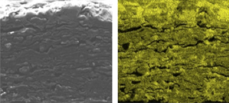
Volume Resistive Paper - 100K - 160GSM


Description
As part of technical raw material developed and experienced since 2006 for electronic application, the conductive paper 1K has especially been designed as electrode layers for the custom fabrication of touch sensors and especially force sensing resistors.
It can also be used for its piezoresistive behavior under compression but the conductive paper 100K is more interesting for such applications.
This paper was also used for the design of anti-static or shielding materials, heat power transfer, temperature and humidity sensing or else as an electrode or functional layer in various components such as power sources.
Technical Details
This paper ca be disposed as standard sheets (A5, A4 or 1 Foot Square) or else as bigger sheets on request. The PLK-1K paper was intensively studied and we can provide the following specifications for our current stock:
Electrical Specifications
| TF Surface Resistance | 44.1 KOhms / Sq +/- 10% | |
| BF Surface Resistance |
|
|
| Electrical Volume Resistance | 0.7 * 10-5 Ohms.m | |
| Single page variability | < 5% | |
| Page to Page variability | < 10% | |
| Max Power |
5 Watts |

Paper Specifications
| Weight | 100 g/m2 |
| Thickness | 140 microns |
| Bulk | 0.71 g/cm3 |
| Roughness TF | 10 microns |
| Roughness BF | 7 microns |
| Cobb Water (60s) | 50+ g/m2 |
Recycling
This product was made in Europe mostly from wood and cotton fibers. It also contains less than 25% conductive Carbon Pigments and a few percent chemical additives.
It can (ands should) be disposed in recycling beans. Simply leave it free from other bonded materials such as metal connectors or plastic cover.
It was also optimized to have a minimal impact when buried, burnt or lost in the wild: it is biodegradable over time and burns much more easily than synthesis polymers.
Adding carbon-based or other electrically conducting particles into the paper pulp prior to producing a paper or a molded object enables to produce various types of electro-functional layers with varying degrees of properties, among which electrically relative surface and volume conductivity.
We have extended expertise on the conception to manufacturing of such specialty papers and we are able to provide resources and lead the production of a variety of components with expert manufacturers world-wide.
Past and current portfolio include experiencing developments on: resistors, sensors and other components and circuits such as RC filters, semi-conductors, piezoelectric, heating transducers, batteries, photovoltaic and other solar enegy acquisition systems.
Most electronic components can thus be made of local, renewable and recycled resources
and they can be biodegradable and compostable.
Encapsulation Variable
External layers, laminates and encapsulation systems are added to wrap and protect de core from external strain
Depending on the application, the choice for the wrapping material and process to be favored can be very different from one application to another.
Our most standard and universal solution for recycled goods exploits thin layers of pure thermoplastics layers sealing components on the edges. The core remains most unbounded inside and the whole can efficiently be separated and put into the recycle bin or also shredded by modern industrial equipment for electronics parts recycling.
Such differences with fully plastic-based electronics represent huge improvements in terms of electronics recycling and waste management.
Towards a single machine and process for mass production
Wile currently requiring a series of productions at papermakers, then printers and then converters in electronics, papierlogik has been working for long on developments involving the used of a single customized paper-machine integrating printers and converting lines.
Such a solution can be developed today and produced efficiently in the future, yet for a substantial cost, but this would enable the production of considerably cleaner electronics than most of what is being produced today.
With AI, we are able to design much more efficiently a machine that will be at the same time easy to modify and setup and that will enabled better monitoring and production quality and speed.
We have shown the industrial potential for such developments with various customers and parnters, among which MOOS in the Netherlands, for the fast and efficient production and implementation of force-sensor arrays counting objects for atomated Stock Management systems.
Printed electronics : Guthenberg remains on page
Printing electronic components just like you would print colored layer on a sheet has been an active field of research since at least the 1950's, and conventionnal printing processes such as screen printing have been used since at least the 1980's to mass produce certain types of electronic components.
In labs, you can find research and prototypes of nearly any kind of micro-electronic components developped using these techniques. However, and even if they can lead to massive cost-reductions when well mastered, this takes highly experiences operators and other process technologies such as etching or PVD are still not as fast yet, but they can deliver better quality and finer resolution especially below the micron order.
Thus, if producing a chip does not make much sense, we can however produce most of the remaining with printed technologies and solder or glue components that were an not able to print.